Trying to build a 6502 based computer.
We have (see previous chapter) a 6502 in free run: it executes NOP, NOP, NOP, ... and by inspecting the address lines (either having LEDs on the high lines, or using the scope on the low lines) we observe the addresses change. But are we sure the 6502 is doing what we expect? Would be nice if we can check that.
Then I had a nice idea: the Nano controls the clock, so it knows when the address bus is valid, can't the Nano snoop the address bus? Can't we snoop (read) the data bus as well? Can't we write the data bus? Yes, yes, and yes.
We will do the following experiments
- 2.1. Clock - Use Nano as clock
- 2.2. Address bus - Use Nano to trace the address bus
- 2.3. Jump loop - Test case: trace a JMP loop
- 2.4. Data bus - Use Nano to trace the data bus as well
- 2.5. Interrupt (IRQ) - Test case: trace a single IRQ
- 2.6. Emulate ROM - Use Nano to respond to data read requests
- 2.7. Emulate RAM - Use Nano to also respond to data write requests
- 2.8. Test IRQ - Test case: trace IRQs
- 2A.1. 2560 Shield - Using a Mega 2560
- 2A.2. Testing the shield - Sketches for the shield
- 2A.3 Memory - Sketch emulating memory
The first step was taken in the previous chapter. We used a Nano as a clock source for the 6502. And that's all the Nano did. The address lines of the 6502 are dangling, the data lines of the 6502 are hardwired to EA (the opcode of the NOP instruction).
The Nano runs a simple sketch that flips the clock line, and behold we have a 6502 "free" running at 160kHz.
With the first experiment, we believe the 6502 is executing NOPs. Can we check that? Can we check that it starts at EAEA (the reset vector at FFFC and FFFD also reads EA and EA) and then progressing to EAEB, EAEC? Can we spy (read) the address bus?
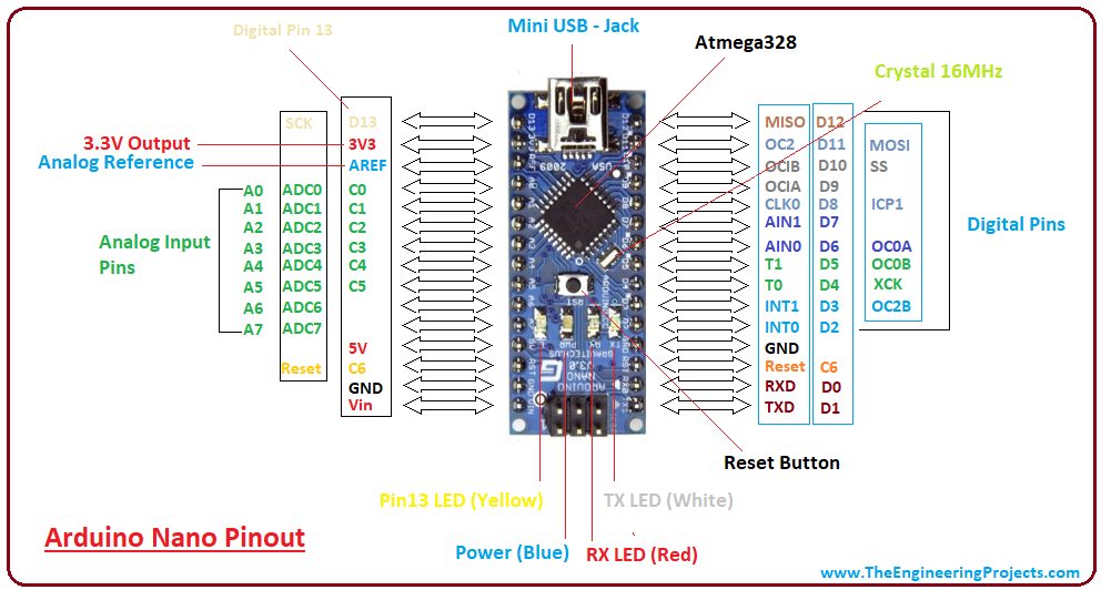
Since the Nano generates the clock, we know when we have to sample the address bus. Does the Nano have enough inputs? It seems to have D0..D13 so 14 lines. However D0 and D1 double as RXD and TXD and we need those two pins to send the trace to the PC (over USB). That leaves us with 12 lines, where 16 would be nice. From the pinout we see that analog pins A0..A5 also have a double role, they can act as digital pins. That's 6 more digital pins.
In other words, we have 18 digital pins. We need 1 for clock and 16 for the address lines. Even one spare. Let's connect:

The schematics above looks like this on my breadboard:

The program on the Nano, AddrSpy6502 is simple. The loop() pulses the clock, reads all 16 address lines and prints them out in hex (with a time stamp).
void loop() {
  // Send clock low
  digitalWrite(PIN_CLOCK, LOW);
  // Send clock high again
  digitalWrite(PIN_CLOCK, HIGH);

  // Read address bus
  uint16_t addr=0 ;
  addr += digitalRead(PIN_ADDR_0 ) << 0;
  addr += digitalRead(PIN_ADDR_1 ) << 1;
  ...
  addr += digitalRead(PIN_ADDR_15) << 15;

  // Print address bus
  char buf[32];
  sprintf(buf,"%9ldus %04x",micros(),addr);
  Serial.println(buf);
}
This is the experiment I did.
- I pressed the reset button of the Nano down, and with the same hand I pressed the reset button of the 6502 down.
- I cleared the output of the Arduino terminal.
- I released the reset of the Nano.
- As soon as I saw the first output of the Nano, I released the reset of the 6502.
- I disabled auto-scroll in the terminal and copied the trace.
This was the trace (I manually added the <- reset released).
Welcome to AddrSpy6502
      400us 3586
      828us 3586
     1264us 3586
     1704us 3586
     2928us 3586
     4460us 3586
     5988us 3586
     7520us 3586
        ...
   406848us 3586
   408380us 3586
   409908us 3586 <- reset released
   411440us 3586
   412968us 01ee
   414500us 01ed
   416028us 01ec
   417556us fffc
   419088us fffd
   420620us eaea
   422148us eaeb
   423680us eaeb
   425208us eaec
   426740us eaec
   428268us eaed
   429800us eaed
   431328us eaee
   432860us eaee
   434388us eaef
   435916us eaef
   437448us eaf0
   438980us eaf0
   440508us eaf1
Note that the first ~400 000 us of the Nano trace, the 6502 was still in reset. It had a random value on the address bus, in this case 3586 (hex). Just before 409908us I released the reset of the 6502 (you can't see that, it's my guess).
What we see on the address bus after reset can be found in the 6502 datasheet, but is also very well explained on the 6502.org site. There are 7 clock ticks before our program starts: first two internal [I] ticks, then three stack [S] ticks, and finally two vectored [V] jump ticks:
                 // 6502 reset released
   409908us 3586 // (1) [I] first internal administrative operation of 6502
   411440us 3586 // (2) [I] second internal operation
   412968us 01ee // (3) [S] push of return address (PCH) on stack, decrement stack pointer S (was EE)
   414500us 01ed // (4) [S] push the return address (PCL) on stack, decrement stack pointer S (was ED)
   416028us 01ec // (5) [S] push the processor status word (PSW) on stack, decrement stack pointer S (was EC)
   417556us fffc // (6) [V] get PCL from reset vector (FFFC), presumably reads EA
   419088us fffd // (7) [V] get PCH from reset vector (FFFD), presumably reads EA
   420620us eaea // Fetches 1st instruction (NOP) - after jump via reset vector, indeed EAEA.
   422148us eaeb // Executes 1st instruction (NOP)
   423680us eaeb // Fetches  2nd instruction (NOP)
   425208us eaec // Executes 2nd instruction (NOP)
   426740us eaec // Fetches  3rd instruction (NOP)
Some notes:
- All three interrupts, NMI with vector at FFFA, RESET with vector at FFFC and IRQ with vector at FFFE have the same 7-clock interrupt sequence.
- One exception: for RESET the three pushes are fake: the 6502 issues a read to the stack memory instead of a write.
- The stack pointer (S) has a random value after reset, in the above run it happened to be EE. The stack page (high byte) is hardwired to 01 on the 6502 (0100-01FF).
- The stack operation are pushes (which are patched to read instead of write), and on the 6502 the stack grows downwards. So, the stack access is on 01EE, 01ED, and 01EC.
- We see the vector load at FFFC and FFFD.
- We see the first instruction at EAEA (since all memory location contain EA, so do the vector addresses at FFFC and FFFD).
- A NOP is two cycles, and we see that after RESET the address bus indeed changes every other step.
- It might seem like the first NOP takes only 1 cycle; the
eaeaappears only once on the address bus. See note below for explanation. - The time between the trace lines (one clock period) is about 1500us, so we are running at 0.7kHz
Cycle explanation The 6502 actually has a 3-stage pipeline: fetch, decode, execute. The NOP instruction uses implied addressing. This is very well explained in the Programming manual. I quote
Implied addressing is a single-byte instructions. [...] Operations of this form take 2 clock cycles to execute. The first cycle is the OP CODE fetch and during this fetch, the program counter increments. In the second cycle, the incremented PC-counter is now the address of the next byte of the instruction. However since the OP CODE totally defines the operation [Maarten: there is no second byte for an operand], the second memory fetch is worthless and any PC-counter increment in the second cycle is suppressed. During the second cycle, the OP CODE is decoded with recognition of its single byte operation. In the third cycle, the microprocessor repeats the same address to fetch the next OP CODE. This is the second time the memory address is fetched: once as second byte of the first instruction and second, as the correct OP CODE of the next instruction.
This is my version of the implied addressing mode table in the Programming manual.
| cycle | address | data | 1 fetch | 2 decode | 3 execute | comment |
|---|---|---|---|---|---|---|
| 1 | PC | OPCODE1 | OPCODE1 | OPCODE0 | Fetch new (OPCODE1), execute previous (OPCODE0) | |
| 2 | PC+1 | OPCODE2 | OPCODE2 | OPCODE1 | Ignore OPCODE2 (is not operand), do not step PC | |
| 3 | PC+1 | OPCODE2 | OPCODE2 | OPCODE1 | Fetch new (OPCODE2), execute previous (OPCODE1) |
Which means that for our all-NOPs program, it pans out as follows.
| cycle | address | data | fetch | decode | execute | comment |
|---|---|---|---|---|---|---|
| 1 | EAEA | NOP1 | NOP1 | Empty pipeline after reset | ||
| 2 | EAEB | NOP2 | (NOP2) | NOP1 | Ignore NOP2, do not step PC | |
| 3 | EAEB | NOP2 | NOP2 | NOP1 | Fetch NOP2, execute NOP1 | |
| 4 | EAEC | NOP3 | (NOP3) | NOP2 | Ignore NOP3, do not step PC | |
| 5 | EAEC | NOP3 | NOP3 | NOP2 | Fetch NOP3, execute NOP2 | |
| 6 | EAED | NOP4 | (NOP4) | NOP3 | Ignore NOP4, do not step PC |
The previous experiment is a success: we see the address lines increment nicely (in steps of two) and also the reset behavior is as documented. Still, it would be nice to have a more realistic program; a series of NOPs is not very convincing.
However, without a memory to store our program, we are limited in our possibilities. There is one way out: go old style. Write a program in hardware.
I got the idea from James Calvert's tight loop. We make some logic (in hardware) that emulates an 8 byte program. We NOR together the first three address lines to create the, let's call it, "v-signal". This v-signal is input to D2, D3 and D6 of the 6502, the other data lines (D0, D1, D4, D5 and D7) are bound to GND. So, the data bus is wired to 0b 0v00 vv00 depending on the value of v. This means that
- if v=0 then D = 0b 0000 0000 = 0x00
- if v=1 then D = 0b 0100 1100 = 0x4C
For the various addresses, that gives the following data reads:
| address (hex) | address (bin) | v-signal | data | comment |
|---|---|---|---|---|
| FFFC | ... 100 | 0 | 00 | RST vector 0000 |
| FFFD | ... 101 | 0 | 00 | RST vector 0000 |
| FFFE | ... 110 | 0 | 00 | (don't care) |
| FFFF | ... 111 | 0 | 00 | (don't care) |
| 0000 | ... 000 | 1 | 4C | JMP 0000 |
| 0001 | ... 001 | 0 | 00 | JMP 0000 |
| 0002 | ... 010 | 0 | 00 | JMP 0000 |
| 0003 | ... 011 | 0 | 00 | (don't care) |
In other words, at FFFC, the 6502 reads the start address 00 00, and at 0000 the 6502 reads 4C 00 00. Note that 4C 00 00 means JMP 0000, since 4C is the opcode for JMP absolute.
How do we implement this in hardware? This the schematic:

Here is a photo of my board. Note the triple OR (4075) and the hex inverter (7404) chips on the right. Also note the three blue wires coming in (from A0, A1, A2) and the blue wire going out (to D2, D3 and D6).

With the same sketch as the previous experiment, let's make a trace again. We repeat our manual steps: Nano reset down, 6502 reset down, Nano reset up, wait for output, 6502 reset up. This is the trace (I manually added the <- reset released again):
Welcome to AddrSpy6502
      400us 0001
      820us 0001
     1248us 0001
     1676us 0001
        ...
   263028us 0001
   264560us 0001
   266088us 0001
   267620us 0001
   269148us 0001
   270680us 0001 <- reset released
   272208us 0001
   273740us 01fa
   275268us 01f9
   276800us 01f8
   278328us fffc
   279856us fffd
   281388us 0000
   282920us 0001
   284448us 0002
   285980us 0000
   287508us 0001
   289040us 0002
   290568us 0000
   292100us 0001
   293628us 0002
Some notes
- Just before 270680us the reset is released (can't see that from the trace).
- We see the two internal administrative operations.
- We see the (fake) push of PCH, PCL, PSW. The stack pointer S now starts at FA, so pushes to 1FA, 01F9 and 01F8.
- We see the reset vector load (FFFC, FFFD).
- At 281388us, we see the load of 0000 (this confirms that FFFC and FFFD read 00 00).
- We see the load of 0001, 0002.
- We see the load of 0000 again, which suggests that JMP 0000 was executed.
- One clock period is still about 1500us (0.7kHz)
In the notes on the previous experiment, we have "load of 0000 (this confirms that FFFC and FFFD read 00 00)". Wouldn't it be nice if we could not only see the address bus, but also the data bus? We can, but we loose details on the address bus.
Recall that we have Nano D2 for the 6502 ϕ0 (clock), and Nano D4..D13 plus A0..A5 for 6502 A0..A15. This leaves Nano D3, A6 and A7 free. Let's redesign;
- Leave Nano D2 to 6502 ϕ0 (clock).
- Connect Nano D3 to 6502 R/nW so that we can trace if the 6502 did a read or a write on the data bus.
- Use Nano D4..D11 for 6502 data bus D0..D7. Full data trace.
- Use Nano D12, D13, A0..A7 for 6502 A0..A9. Thus 10 bit address trace.

Find below my breadboard version. I still have the JMP loop circuit (3-input OR with inverter) on the right.

There is one problem with this wiring: Nano A6 and A7 are analog only. We cannot use digitalRead() on those pins. We can however read them in an analog fashion by using analogRead() and comparing the result with half the maximum analog readout: 1024/2. The drawback is that analogRead() is slow:
On ATmega based boards (UNO, Nano, Mini, Mega), it takes about 100 microseconds (0.0001 s) to read an analog input, so the maximum reading rate is about 10,000 times a second.
We prefer to use 10 bits, because this means we have 4 pages (a 6502 page is 256 bytes):
- Page 0, for well, zero-page addressing of the 6502.
- Page 1, for the stack (hardwired on page 1 by the 6502).
- Page 2, for the code.
- Page 3, for the interrupt vectors (hardwired to FFFx by the 6502).
The result is a memory map with 4 pages of each 256 bytes (so 1kB in total), that is mirrored 64 times:

The associated Arduino sketch, now also captures R/nW and the data pins:
void loop() {
  // Send clock low
  digitalWrite(PIN_CLOCK, LOW);
  // Send clock high again
  digitalWrite(PIN_CLOCK, HIGH);

  // Read address bus
  uint16_t addr=0 ;
  addr += digitalRead(PIN_ADDR_0) << 0;
  addr += digitalRead(PIN_ADDR_1) << 1;
  ...

  // Read R/nW
  uint16_t rnw=0 ;
  rnw += digitalRead(PIN_RnW) << 0;

  // Read data bus
  uint16_t data=0 ;
  data += digitalRead(PIN_DATA_0) << 0;
  data += digitalRead(PIN_DATA_1) << 1;
  ...

  // Print address bus
  char buf[32];
  sprintf(buf,"%9ldus %03x %0x %02x",micros(),addr,rnw,data);
  Serial.println(buf);
}
We made a trace of the JMP 0000 program in the same way as before (just after reset):
Welcome to AddrDataSpy6502
      752us 002 1 00
     1504us 002 1 00
     2264us 002 1 00
     3024us 002 1 00
        ...
   376984us 002 1 00
   378856us 002 1 00 <- reset
   380736us 002 1 00
   382608us 1fd 1 00
   384464us 1fc 1 00
   386336us 1fb 1 00
   388216us 3fc 1 00
   390088us 3fd 1 00
   391944us 000 1 4c
   393816us 001 1 00
   395696us 002 1 00
   397568us 000 1 4c
   399424us 001 1 00
   401296us 002 1 00
   403176us 000 1 4c
   405048us 001 1 00
   406904us 002 1 00
- Since we capture only 10 address lines, we only print 3 nibbles.
- The first nibble of the address bus is only 0, 1, 2 or 3 (we only capture 2 bits in this nibble).
- Since we still have the JMP loop wired, all accessed memory locations read as 00 except location 0000, which reads 4C.
- The three push instructions (01fd, 01fc, 01fb) are indeed fake: they read instead of write (R/nW flag is 1 - do we trust that, it's always 1).
- One clock period is now just below 2000us (0.5kHz).
We should be able to generate an interrupt. The IRQ line on the board is pulled up, so if we add a wire and touch the GND signal, we should get an interrupt.
Intermezzo on interrupts
The 6502 IRQ line is not edge but level sensitive: a low level causes an interrupt. The IRQ line is sampled at the end of each instruction. There are three possible cases.
(1) If the line is high, no interrupt request is pending and the 6502 runs the next instruction till completion, before it samples the IRQ line again.
(2) If the IRQ line is low, an interrupt request is pending. If the I flag ("IRQ-disable") in the program status word is set, the interrupt is not taken; the 6502 runs the next instruction till completion before it samples the IRQ line (and I flag) again.
(3) If the IRQ line is low and the I flag is clear, the interrupt sequence will be initiated. The Program Counter (PC, high and low byte) and the Processor Status Word (PSW) are pushed onto the stack and the IRQ-disable flag (I) is set disabling further interrupts. The Program Counter Low is loaded from FFFE and the Program Counter High from FFFF. The vector at FFFE/FFFF points to the start of the so-called Interrupt Service Routine (ISR), which thus now starts to execute.
The ISR should do the proper action for the interrupt, but also some administrative work: it should signal the device that pulled the IRQ line low, that it is serviced, so that it will let the IRQ line go high again. The ISR ends with a Return from Interrupt (RTI) instruction. This restores the I flag (clearing it) and a new interrupts can be handled. If the (I) flag is cleared inside the ISR routine, nested interrupts can occur.
So, if we pull IRQ low for a moment, the ISR will be executed (assuming I=0). This means the the main program (the JMP loop at 0000) is pre-empted and that the 6502 will start executing ... 0000 (because FFFE and FFFF both store 00).
We will see the interrupt sequence! Another interesting observation is that our ISR never returns. It loops back to 0000 and never executes a RTI. So after the first interrupt I=1, and no new interrupts will be serviced. That is, till the next RESET.
Let's give it a try. Lets run the tracer and short circuit the nIRQ line of the 6502 with GND for a brief moment.
 62728408us 000 1 4c
 62730280us 001 1 00
 62732136us 002 1 00
 62734016us 000 1 4c
 62735888us 001 1 00
 62737744us 002 1 00 <- IRQ
 62739632us 000 1 4c
 62741496us 000 1 4c
 62743368us 100 0 00
 62745224us 1ff 0 00
 62747096us 1fe 0 00
 62748976us 3fe 1 00
 62750848us 3ff 1 00
 62752704us 000 1 4c
 62754576us 001 1 00
 62756456us 002 1 00
 62758328us 000 1 4c
 62760184us 001 1 00
 62762056us 002 1 00
- We see the 6502 looping JMP 0000 calls (e.g. at 62728408us and another at 62730280us).
- At 62737744us there is the IRQ (you can not see that from this line).
- We have the two internal cycles.
- We have the 3 pushes (to 100, 1ff, 1fe).
- Note the the 3 pushes indeed have the R/nW flag 0 (first time, jaayy)
- We have a read from 3fe (FFFE) and 3ff (FFFF), the IRQ vector (remember we capture only 12 address bits).
- Next, the program counter switches to 000.
- A second touch of the wire did not cause a second FFFE/FFFF lookup (presumably because I is now set).
- I think we were lucky: we started with I cleared. I now believe that a 6502 reset does not guarantee this.
Success, interrupt fully matches our model.
The Nano now controls the clock of the 6502, but it also reads the (well, most) address lines. And it is connected to the data lines. What prevents us from writing a sketch that has a 1k array (remember we capture 10 address lines which can address 1024 locations), indexes that array with the received address, retrieves the byte at that location, and write the value of that byte to the data lines?
Nothing. This basically implements a ROM.
Just a ROM for now, in the next section we go one step further and emulate RAM too.
Since the Nano now writes to the data lines in addition to the 6502, there is a risky situation: if one writes 0 and the other writes 1, we get a short circuit. So I decided to add (1k) resistors on the line. A 5V short then causes a 5mA current. Hope both chips can handle that. A 10k felt too high for me.

I used an extra breadboard to insert the 1k resistors in the data lines:

The associated Arduino sketch, now looks up the data and writes it on the data lines:
void loop() {
  // Send clock low
  digitalWrite(PIN_CLOCK, LOW);

  // Read address bus
  uint16_t addr=0 ;
  addr += digitalRead(PIN_ADDR_0) << 0;
  addr += digitalRead(PIN_ADDR_1) << 1;
  ...

  // Read R/nW
  uint16_t rnw=0 ;
  rnw += digitalRead(PIN_RnW) << 0;

  // Write data bus
  uint16_t data= mem[addr] ;
  digitalWrite(PIN_DATA_0, (data&(1<<0))?HIGH:LOW );
  digitalWrite(PIN_DATA_1, (data&(1<<1))?HIGH:LOW );
  ...

  // Send clock high again
  digitalWrite(PIN_CLOCK, HIGH);

  // Print address bus
  char buf[32];
  sprintf(buf,"%9ldus %03x %0x %02x",micros(),addr,rnw,data);
  Serial.println(buf);
}
The mem array that is used to lookup data is a byte array that is initialized by calling load() from setup().
uint8_t mem[1024];

void load() {
  // Fill entire memory with NOP
  for(int i=0; i<1024; i++ ) mem[i]=0xEA; // NOP

  // * = $0200
  mem[0x3fc]= 0x00;
  mem[0x3fd]= 0x02;
  // 0200        LDX #$00        A2 00
  mem[0x200]= 0xA2;
  mem[0x201]= 0x00;
  // 0202 LOOP   INX             E8
  mem[0x202]= 0xE8;
  // 0203        STX $0155       8E 55 01
  mem[0x203]= 0x8E;
  mem[0x204]= 0x55;
  mem[0x205]= 0x01;
  // 0206        JMP LOOP        4C 02 02
  mem[0x206]= 0x4C;
  mem[0x207]= 0x02;
  mem[0x208]= 0x02;
}
In case you wonder where this code is coming from. I wrote a simple assembler program that constantly increments X and stores it on location 155 (not wise, since that is in the stack area, but hey, we don't need stack right now). This is the assembler code.
* = $0200
0200        LDX #$00        A2 00
0202 LOOP   INX             E8
0203        STX $0155       8E 55 01
0206        JMP LOOP        4C 02 02
I used the on-line 6502 compiler to get the opcodes. Do not forget the reset vector at 3fc and 3fd.
This is the trace (the <- comments are from me)
Welcome to Rom6502
     1132us 206 1 4c
     1892us 206 1 4c
     2660us 206 1 4c
        ...
   312740us 206 1 4c
   314588us 206 1 4c
   316468us 206 1 4c
   318348us 206 1 4c <- reset
   320220us 206 1 4c
   322068us 1ab 1 ea
   323940us 1aa 1 ea
   325828us 1a9 1 ea
   327708us 3fc 1 00
   329548us 3fd 1 02
   331420us 200 1 a2 <- main
   333308us 201 1 00
   335180us 202 1 e8 <- loop
   337028us 203 1 8e
   338900us 203 1 8e
   340788us 204 1 55
   342660us 205 1 01
   344508us 155 0 ea <- save X
   346380us 206 1 4c
   348268us 207 1 02
   350140us 208 1 02
   351988us 202 1 e8 <- loop
   353860us 203 1 8e
   355748us 203 1 8e
   357620us 204 1 55
   359476us 205 1 01
   361340us 155 0 ea <- save X
   363228us 206 1 4c
   365100us 207 1 02
   366948us 208 1 02
   368820us 202 1 e8 <- loop
   370716us 203 1 8e
- After reset, the 6502 jumps to main at 200.
- It executes the
LDX #$00(A2 00) and then moves to the start of the loop. - In the loop, it increments X
INX(E8). - Then executes the store of X to 155
STX $0155which takes four ticks 8E 8E 55 01. - In the next clock tick, the 6502 attempts to write. We see address 155 and R/nW at 0 (write). However, our "ROM" (the Nano) ignores the write request. The Nano actually writes
EAitself, causing the dreaded short circuit (but we are rescued by the resistors). - Finally there is the jump to loop
JMP 0202(4C 02 02).
Let's support writing.
In the previous section we implemented a ROM: the 6502 could read bytes. Those bytes come from a memory array inside the Nano. In this section we will extend the Nano firmware. It will accept writes from the 6502; the written bytes will be written to memory array inside the Nano.
The schematics and breadboard do not change; it is just the firmware ram6502 inside the Nano . This is the important part:
void loop() {
  // Send clock low
  digitalWrite(PIN_CLOCK, LOW);

  // Read address bus
  uint16_t addr=0 ;
  addr += digitalRead(PIN_ADDR_0) << 0;
  addr += digitalRead(PIN_ADDR_1) << 1;
  ...

  // Read R/nW
  uint8_t rnw=0 ;
  rnw += digitalRead(PIN_RnW) << 0;

  // Send clock high again
  digitalWrite(PIN_CLOCK, HIGH);

  // Write or read depends on R/nW
  uint8_t data;
  if( rnw ) { // R/nW==1, so 6502 reads, so Nano writes
    data= mem[addr];
    data_write(data);
  } else { // R/nW==0, so 6502 writes, so Nano reads
    data= data_read();
    mem[addr]= data;
  }

  // Print address bus
  char buf[32];
  sprintf(buf,"%9ldus %03x %0x %02x",micros(),addr,rnw,data);
  Serial.println(buf);
}
Those who have been following my experiments might notice that I'm not consistent with the placement of the clock changes digitalWrite(PIN_CLOCK,LOW) and digitalWrite(PIN_CLOCK,HIGH). The truth is, I do not fully understand what the relation is between the clock edges and the moments to read the address, R/nW line, or access the data lines (see chapter 4 where I studied this in more detail).
I wrote a program that really uses RAM (zero page location 33):
0200        LDA #$00        A9 00
0202        STA *$33        85 33
0204 LOOP
0204        INC *$33        E6 33
0206        JMP LOOP        4C 04 02
The load() routine in Arduino sketch is thus (again, remember to set the reset vector):
void load() {
  // Fill entire memory with NOP
  for(int i=0; i<1024; i++ ) mem[i]=0xEA; // NOP

  // RAM is preloaded with a simple programm
  //   https://www.masswerk.at/6502/assembler.html
  // * = $0200
  mem[0x3fc]= 0x00;
  mem[0x3fd]= 0x02;
  // 0200        LDA #$00        A9 00
  mem[0x200]= 0xA9;
  mem[0x201]= 0x00;
  // 0202        STA *$33        85 33
  mem[0x202]= 0x85;
  mem[0x203]= 0x33;
  // 0204 LOOP
  // 0204        INC *$33        E6 33
  mem[0x204]= 0xE6;
  mem[0x205]= 0x33;
  // 0206        JMP LOOP        4C 04 02
  mem[0x206]= 0x4C;
  mem[0x207]= 0x04;
  mem[0x208]= 0x02;
}
This is the trace:
Welcome to Ram6502
Memory loaded
     1248us 314 1 ea
     2048us 001 1 ea
     2848us 001 1 ea
     ...
   394464us 001 1 ea    <- RESET
   396324us 001 1 ea    // Internal
   398200us 001 1 ea    // Internal
   400072us 100 1 ea    // Push PCH
   401928us 1ff 1 ea    // Push PCL
   403808us 1fe 1 ea    // Push PSW
   405680us 3fc 1 00    // LD PCL
   407536us 3fd 1 02    // LD PCH
   409408us 200 1 a9 // LDA #$00
   411280us 201 1 00
   413160us 202 1 85 // STA *$33
   415032us 203 1 33
   416888us 033 0 00    <- store 0 in 33
   418760us 204 1 e6 // INC *$33
   420640us 205 1 33
   422496us 033 1 00    <- gets 0 from 33
   424368us 033 1 00
   426240us 033 0 01    <- store 1 in 33
   428124us 206 1 4c // JMP 0204
   429976us 207 1 04
   431848us 208 1 02
   433720us 204 1 e6 // INC *$33
   435600us 205 1 33
   437472us 033 1 01    <- gets 1 from 33
   439332us 033 1 01
   441200us 033 0 02    <- store 2 in 33
   443080us 206 1 4c
   444936us 207 1 04
   446816us 208 1 02
The clock steps are still 2000us or 0.5kHz.
Now that we have RAM operational, we can really test interrupts. We did that before (by grounding nIRQ), but we could do that only one time (after reset). The reason is that as part of the IRQ handling (the 7 steps of interrupt handling), the 6502 automatically sets the I flag (also known as IRQ-disable flag) to 1. From that moment on, IRQs are disabled.
The I flag is cleared by the RTI instruction, since that pops the old PSW register (which contains the I flag). Now that we have RAM emulation, the push of PSW is operational, so the pop of PSW is effective.
The new Nano sketch ramirq6502 is identical to the previous ram6502 with two exceptions. The mem[] array is loaded with a different "program" for the 6502. And we have added a mem_dump() routine that is called from setup() so that we can check the mem[] array is correctly initialized.
The core of the change is the new 6502 "program". There are two functions main and isr. The main gets executed from the reset vector.
* = $0200
0200 MAIN
0200        CLI             58
0201        LDA #$00        A9 00
0203        STA *$33        85 33
0205        STA *$44        85 44
0207 LOOP
0207        INC *$33        E6 33
0209        JMP LOOP        4C 07 02
Function main has a loop that increments zero page location 33.
Before the loop, main initializes zero page location 33 to 00. It has two other initializations: zeroing page location 44 to 00, and enabling of interrupts (CLI). The enabling of interrupts allows the second function isr to be called when grounding the nIRQ line. The isr routine increments zero page location 44. The function isr is not called from main, it gets executed from the irq vector.
* = $0300
0300 ISR
0300        INC *$44        E6 44
0302        RTI             40
The opcodes of both functions are written to the mem[] array in mem_load(). Do not forget that mem_load() should initialize mem[] locations fffc/fffd (reset) and fffe/ffff (irq) as well.
This is the annotated trace (note the mem dump at the top).
Welcome to RamIrq6502
200: 58 a9 00 85 33 85 44 e6 33 4c 07 02 ea ea ea ea
300: e6 44 40 ea ea ea ea ea ea ea ea ea ea ea ea ea
3f0: ea ea ea ea ea ea ea ea ea ea ea ea 00 02 00 03
Memory loaded
    12192us 2f1 1 ea
    13904us 2f1 1 ea
    15776us 2f1 1 ea
        ...
   290664us 2f1 1 ea
   292536us 2f1 1 ea <- reset
   294416us 2f1 1 ea    // internal
   296288us 2f1 1 ea    // internal
   298144us 139 1 ea    // push PCH
   300016us 138 1 ea    // push PCL
   301896us 137 1 ea    // push PSW
   303752us 3fc 1 00    // LD PCL
   305624us 3fd 1 02    // LD PCH
   307496us 200 1 58 <- main
   309376us 201 1 a9
   311248us 201 1 a9
   313104us 202 1 00
   314976us 203 1 85
   316856us 204 1 33
   318728us 033 0 00 <- clear 33
   320588us 205 1 85
   322456us 206 1 44
   324336us 044 0 00 <- clear 44
   326192us 207 1 e6 <- loop
   328064us 208 1 33
   329952us 033 1 00
   331820us 033 1 00
   333672us 033 0 01 <- update 33
   335544us 209 1 4c
   337416us 20a 1 07
   339296us 20b 1 02
   341152us 207 1 e6 <- loop
   343024us 208 1 33
   344896us 033 1 01
   346776us 033 1 01
   348632us 033 0 02 <- update 33
   350504us 209 1 4c
   352376us 20a 1 07
   354256us 20b 1 02
        ...
  1741784us 209 1 4c
  1743656us 20a 1 07
  1745536us 20b 1 02
  1747408us 207 1 e6
  1749264us 208 1 33
  1751140us 033 1 5f
  1753016us 033 1 5f
  1754888us 033 0 60 <- IRQ (when PC=209)
  1756744us 209 1 4c    // internal
  1758616us 209 1 4c    // internal
  1760496us 136 0 02    // push PCH
  1762372us 135 0 09    // push PCL
  1764224us 134 0 60    // push PSW
  1766096us 3fe 1 00    // LD PCL
  1767976us 3ff 1 03    // LD PCH
  1769848us 300 1 e6 <- ISR
  1771704us 301 1 44
  1773580us 044 1 00
  1775456us 044 1 00
  1777328us 044 0 01 <- update 44
  1779184us 302 1 40 <- RTI
  1781064us 303 1 ea    // internal
  1782936us 133 1 ea    // internal
  1784808us 134 1 60    // pop PSW
  1786664us 135 1 09    // pop PCL
  1788536us 136 1 02    // pop PCH
  1790416us 209 1 4c <- back in main
  1792288us 20a 1 07
  1794148us 20b 1 02
  1796016us 207 1 e6 <- loop
  1797896us 208 1 33
  1799768us 033 1 60
  1801624us 033 1 60
  1803496us 033 0 61 <- update 33
  1805380us 209 1 4c
  1807248us 20a 1 07
  1809104us 20b 1 02
The 6502 uses a post decrement for stack pushes. In other words S points at the "first free" location just beyond the "top" of the stack. But also, the stack grows downwards. A typical initial value for S would be FF (LDX #$ff followed by TXS):

With that in mind let's have a look at the trace
- The first instruction of
mainclears the interrupt disable flagCLI, enabling interrupts. - It would have been wise to initialize the stack pointer. In our run it happens to have initial value 39.
- We see the by now understood 7 step reset sequence. Note that there are three (fake) pushes. Since S happened to be 39, they are to 139, 138, 137. so S is 36 after reset. See figure below.
- When the IRQ comes in we see similar 7 steps. Note that indeed PCH is now pushed at 136, PCL at 135,and PSW at 134, leaving S at 33, see figure below).
- The PC is now loaded from the vector FFFE and FFFF (3FE/3FF in our 10 bit trace).
- This executes the ISR at 300, which increments zero page location 44 to 1.
- The RTI instruction is then executed. This includes 3 pops, which have the opposite behavior: pre increment.
- First the PSW is popped from 134, then PCL from 135 (09), and finally PCH from 136 (02).
- Indeed the next instruction is from 0209.
- It is a pity that we can't see that the I flag is set. The old value (cleared) is pushed at 1764224us, and that same value is popped at 1784808us.

The chapters in the appendix where added later - when I started to develop some PCBs.
The Nano is a great tool for monitoring (and controlling) the 6502, but it has one serious disadvantage: it has too few pins. So, as a last step in the 'Emulation' chapter, I decided to switch from ATmega328 (on the Nano) to ATmega2560. This increases digital pins from 22 to 54 (and also gives us more memory).
| ATmega328 | ATmega2560 | |
|---|---|---|
| Voltage | 5V | 5V |
| Flash | 32kB | 256kB |
| SRAM | 2kB | 8kB |
| Clock | 16MHz | 16MHz |
| Dig pins | 22 | 54 |
| Price | €20 | €35 |
| Clone | €3 | €8 |
| Data sheet |
Note that there are different form factors for ATmega2560 based Arduino boards. The classic one is big (54×102 mm²) because it has (largely) single header rows. The compact one (54×38 mm²) has double header rows. Note that boards come in 3V (instead of 5V) and also without USB (I prefer with USB, I believe they are always 5V). The clones with USB also come with varying "USB to UART" chips (CH340G, CH340C, CP2104) - but here I don't have a preference. Also, boards come with and without soldered headers, I prefer non-soldered, because I want female headers.
I believe the compact ones are tagged with "pro" and the USB ones with "embed", so Google for atmega2560 pro embed.
I made a schematic (using the webtool EasyEDA) with the following considerations:
- I have connected every pin of the 6502 (the "slave") to a pin of the 2560 (the "master").
- The exception being the power pins of the 6502: the GND pins are hardwired and the VCC pin is wired via a transistor (T1) to a pin of the 2560.
- The power of the 2560 and the power of the 6502 (switched via the transistor) have their own signalling LEDs (LEDMPOW and LEDSPOW).
- Even NC pins of the 6502 are connected to the 2560, because newer models of the 6502 (e.g. W65C02) have those pins connected.
- To prevent short circuit (6502 outputs to 5V on the same pin where the 2560 outputs 0V) I have added 2k2 resistors on all pin-pin connections.
- I have tried to order the connections "logically". I connected similar signals to one "port" of the 2560, and I connected the wires of one port in order. For example, all data lines of the 6502 go to port A of the 2560; D0 maps to PA0, D1 to PA1, and ... D7 to PA7.
- I have also added an expansion connector (J1), which breaks-out all pins of the 6502.
- There is also a small expansion header (J2) for power (5V, GND) and an even smaller expansion header (J3) that breaks out two pins of the 2560 (so that in an experiment, we can feed an external event to the 6502).
- There are three general purpose LEDs (LED0, LED1, and LED2). Such a LED can be programmed to e.g. show the generated clock pulse (when it is slow), or act as an output device for the 6502 (writes to 8000 could be mapped to a LED).
- There are also three general purpose switches (SW0, SW1, and SW2). Such a switch can be programmed to give an IRQ or, for example, hand control the clock ticks.
- The plan is that the 6502 gets a ZIF socket, and the 2560 mates with male/female headers.
I planned to make a real shield: the 6502 on top of the 2560. But there were too many wires and too little space, so I didn't manage the routing. They are now side by side:

I ordered a PCB at JLCPCB which are low priced and have good quality (but prices are rising). If you want to also get some PCBs and want to save on routing, here are the Gerber files. Now that I have it in use there are some possible improvements:
- Maybe if I used the bigger (non "pro") version of the Mega2560 a real on-top shield would be possible.
- Maybe I should have added a jumper for pin 1, so that it can be connected to either ground or D39. This way, the shield also supports the W65C02, which uses pin 1 as output instead of GND.
- More buttons? Play/pause, single step, NMI, IRQ, RESET, device for 6502.

I wrote a short sketch to test the hardware: 2560shield-hwtest. It configures all pins, wires EA (NOP) to DATA, starts clocking and forces a RST. Each clock ot prints the address, rw and data lines. This is the output.
2560shield-hwtest

0000 r EA
0000 r EA
0100 W EA
01FF W EA
01FE W EA
FFFC r EA
FFFD r EA
EAEA r EA
EAEB r EA
EAEB r EA
EAEC r EA
EAEC r EA
EAED r EA
EAED r EA
EAEE r EA
The output is as expected: 2 internal clocks, 3 stack clock, load of reset vector (EAEA) and then executing NOPs (EA) from EAEA onwards. Note that the clock is rather slow: 100ms periods or 10 Hz. This works for 65C02, but not for the NMOS variants. Also, it seems the 65C02 initializes the S register (stack pointer): the trace always pushes at 0100. I am a bit surprised to see Writes here - I thought the 6502 was patched to do reads for the pushes in the reset handling.
Observe that the code does not use pinMode and digitalWrite, but rather directly accesses the hardware registers DDR (data direction register), PORT (write) and PIN. This makes the code faster (no need for the function call) especially, because the design of the PCB maps related pins to one "port".
This means that the code to read the data bus, which, on the Nano assembled individual bits
  // Read data bus
  uint16_t data=0 ;
  data += digitalRead(PIN_DATA_0) << 0;
  data += digitalRead(PIN_DATA_1) << 1;
  ...
  data += digitalRead(PIN_DATA_7) << 7;
is now reduced to one register access
data= PORTAI also wrote a sketch that tests the buttons and the LEDs: 2560shield-ctrl. The first button (SW0) functions as pause/continue (of the clock), the second one generates IRQ and the third one a RST. Note that the "pause" keeps the clock high. This works for 65C02, but not for the NMOS variants. This is a trace.
2560shield-ctrl

but : init
led : init

0000 r EA
0000 r EA
0100 W EA
01FF W EA
01FE W EA
FFFC r EA
FFFD r EA
EAEA r EA
EAEB r EA
EAEB r EA
but : RST asserted
EAEC r EA
EAEC r EA
EAEC r EA
but : RST released
EAEC r EA
EAEC r EA
01FD W EA
01FC W EA
01FB W EA
FFFC r EA
FFFD r EA
EAEA r EA
EAEB r EA
but : pause
but : continue
EAEB r EA
EAEC r EA
EAEC r EA
EAED r EA
EAED r EA
EAEE r EA
but : pause
Again, looks good: the reset sequence at power-up, which is repeated when the RST is released. Also note the pause. The IRQ could not be tested, presumable the interrupts are disabled by default. We need to upgrade the sketch so that we can run a real program.
It is time to let the Mega emulate ROM and RAM, just like we did with the Nano. See the sketch 2560shield-mem. I booted it and pressed and released SW1, which generates an IRQ.
This is the trace <-- is annotation by me.
2560shield-mem

but : init
led : init
mem : init

0000 r EA
0000 r EA
0100 W 00
01FF W 00
01FE W 23
FFFC r 00
FFFD r 02
0200 r 58 <-- CLI
0201 r A9 <-- LDA #$00
0201 r A9
0202 r 00
0203 r 85 <-- STA *$33
0204 r 33
0033 W 00
0205 r 85 <-- STA *$44
0206 r 44
0044 W 00
0207 r E6 <-- INC *$33
0208 r 33
0033 r 00
0033 r 00
0033 W 01 <-- 33 updated to 1
0209 r 4C <-- JMP 0207
020A r 07
020B r 02
0207 r E6 <-- INC *$33
0208 r 33
0033 r 01
0033 r 01
0033 W 02 <-- 33 updated to 2
0209 r 4C <-- JMP 0207
020A r 07
020B r 02
0207 r E6  <-- INC *$33
0208 r 33
0033 r 02
but : IRQ asserted <-- but instruction not yet finished
0033 r 02
0033 W 03 <-- 33 updated to 3 (instruction finished)
0209 r 4C <-- interrupt sequence (2 internal ticks)
0209 r 4C
01FD W 02 <-- interrupt sequence (push PCH PCL PSW)
01FC W 09
but : IRQ released
01FB W 21
FFFE r 00 <-- interrupt sequence (load IRQ vector)
FFFF r 03
0300 r E6 <-- INC *$44 ; interrupt service routine start
0301 r 44
0044 r 00
0044 r 00
0044 W 01 <-- 44 updated to 1
0302 r 40 <-- RTI
0303 r EA
01FA r EA <-- POP PSW PCL PCH
01FB r 21
01FC r 09
01FD r 02
0209 r 4C <-- JMP 0207 ; back in main
020A r 07
020B r 02
0207 r E6
(end of doc)