Edge Triggered Interrupts
Note: The example on this page illustrates how you can use an edge triggered interrupt to monitor/count how many times a switch (PF4) has been pressed. The example code will increment "FallingEdges" anytime a falling edge interrupt trigger is invoked. A breakdown of the registers used in the example is listed below.
// NVIC Registers
#define NVIC_EN0_R              (*((volatile unsigned long *)0xE000E100))  // IRQ 0 to 31 Set Enable Register
#define NVIC_PRI7_R             (*((volatile unsigned long *)0xE000E41C))  // IRQ 28 to 31 Priority Register

// Standard GPIO Port Registers
#define GPIO_PORTF_DIR_R        (*((volatile unsigned long *)0x40025400))
#define GPIO_PORTF_AFSEL_R      (*((volatile unsigned long *)0x40025420))
#define GPIO_PORTF_PUR_R        (*((volatile unsigned long *)0x40025510))
#define GPIO_PORTF_PDR_R        (*((volatile unsigned long *)0x40025514))
#define GPIO_PORTF_DEN_R        (*((volatile unsigned long *)0x4002551C))
#define GPIO_PORTF_AMSEL_R      (*((volatile unsigned long *)0x40025528))
#define GPIO_PORTF_PCTL_R       (*((volatile unsigned long *)0x4002552C))

// GPIO Port Interrupt Registers
#define GPIO_PORTF_IS_R         (*((volatile unsigned long *)0x40025404))
#define GPIO_PORTF_IBE_R        (*((volatile unsigned long *)0x40025408))
#define GPIO_PORTF_IEV_R        (*((volatile unsigned long *)0x4002540C))
#define GPIO_PORTF_IM_R         (*((volatile unsigned long *)0x40025410))
#define GPIO_PORTF_RIS_R        (*((volatile unsigned long *)0x40025414))
#define GPIO_PORTF_ICR_R        (*((volatile unsigned long *)0x4002541C))

// Clock Gating Registers
#define SYSCTL_RCGC2_R          (*((volatile unsigned long *)0x400FE108))
NVIC Base Address: 0xE000.E000
- Enable Offsets (pg 132)
- EN0: 0x100 - Interrupt 0-31 Set Enable
- Priority Offset (pg 132)
- PRI7: 0x41C - Interrupt 28-31 Priority
GPIO PORTF (APB) Base Address: 0x4002.5000
-
Port Configuration Offsets (pg 657)
-
GPIODIR: 0x400 - Direction
-
GPIOAFSEL: 0x420 - Alternate Function Select
-
GPIOPUR: 0x510 - Pull-Up Select
-
GPIOPDR: 0x514 - Pull-Down Select
-
GPIODEN: 0x51C - Digital Enable
-
GPIOAMSEL: 0x528 - Analog Mode Select
-
GPIOPCTL: 0x52C - Port Control
-
Edge Triggering Offsets (pg 657)
-
GPIOIS: 0x404 - Interrupt Sense
-
GPIOIBE: 0x408 - Interrupt Both Edges
-
GPIOIEV: 0x40C - Interrupt Event
-
GPIOIM: 0x410 - Interrupt Mask
-
GPIORIS: 0x414 - Raw Interrupt Status
-
GPIOICR: 0x41C - Interrupt Clear
System Control: 0x400F.E000
- Run Mode Clock Gating Control Register 2 (pg 234 & 462)
- RCGC2: 0x108
void EdgeCounter_Init(void){
  SYSCTL_RCGC2_R 		|= 	0x00000020;     // (a) activate clock for port F
  FallingEdges 			 = 	0;              // (b) initialize counter

  GPIO_PORTF_DIR_R 		&= 	~0x10;    		// (c) make PF4 in (built-in button)
  GPIO_PORTF_AFSEL_R 	&= 	~0x10;  		//     disable alt funct on PF4
  GPIO_PORTF_DEN_R 		|= 	0x10;     		//     enable digital I/O on PF4
  GPIO_PORTF_PCTL_R 	&= 	~0x000F0000; 	// configure PF4 as GPIO
  GPIO_PORTF_AMSEL_R 	 = 	0;       		//     disable analog functionality on PF
  GPIO_PORTF_PUR_R 		|= 	0x10;     		//     enable weak pull-up on PF4
  GPIO_PORTF_IS_R 		&= 	~0x10;     		// (d) PF4 is edge-sensitive
  GPIO_PORTF_IBE_R 		&= 	~0x10;    		//     PF4 is not both edges
  GPIO_PORTF_IEV_R 		&= 	~0x10;    		//     PF4 falling edge event
  GPIO_PORTF_ICR_R 		 = 	0x10;      		// (e) clear flag4
  GPIO_PORTF_IM_R 		|= 	0x10;      		// (f) arm interrupt on PF4

  NVIC_PRI7_R 			 = 	(NVIC_PRI7_R&0xFF00FFFF)|0x00A00000; // (g) priority 5
  NVIC_EN0_R 			 = 	0x40000000;     // (h) enable interrupt 30 in NVIC
  EnableInterrupts();           			// (i) Clears the I bit
}
a) Activate clock for Port F:
- Set bit 5 (GPIOF), on the RCGC2 register to activate the clock for Port F.
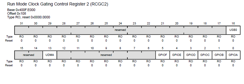
SYSCTL_RCGC2_R |= 0x00000020;
b) Initialize a counter:
- Create a falling edges variable
volatile unsigned long FallingEdges = 0;and set it to 0 FallingEdges = 0;
c) Setup PF4 as input:
- Clear the 4th bit in the GPIODIR register to make it an input

GPIO_PORTF_DIR_R &= ~0x10;- Clear the 4th bit in the GPIOAFSEL register to disable alternate functions

GPIO_PORTF_AFSEL_R &= ~0x10;- Set the 4th bit in the GPIODEN register to make the pin digital enabled

GPIO_PORTF_DEN_R |= 0x10;- Clear bits 16-19 (PMC4) in the GPIOPCTL register to disable peripheral control for PF4

GPIO_PORTF_PCTL_R &= ~0x000F0000;- Write a 0 in the GPIOAMSEL register to disabled analog mode function

GPIO_PORTF_AMSEL_R = 0;- Set the 4rth bit in the GPIOPUR register to enable a weak pull up resistor in the MCU

GPIO_PORTF_PUR_R |= 0x10;
d) Setup PF4 as edge-trigger:
- Clear the 4th bit in the GPIOIS register to have PF4 be edge-sensitive (edge trigger)

GPIO_PORTF_IS_R &= ~0x10;- Clear the 4th bit in the GPIOIBE register so we don't trigger on both the falling and rising edge; interrupt generation will be controlled by the IEV

GPIO_PORTF_IBE_R &= ~0x10;- Clear the 4th bit in the GPIOIEV register to trigger on the falling edge, similarly setting this bit to 1 will have the corresponding bit trigger on a rising edge

GPIO_PORTF_IEV_R &= ~0x10;
e) Clear Flag 4
- Write a 1 to the 4th bit in the GPIOICR register to clear the interrupt flag (acknowledge)

GPIO_PORTF_ICR_R = 0x10;
f) Arm interrupt on PF4:
- Set the 4th bit in the GPIOIM register to arm the interrupt. This will send the corresponding pins interupt to the interrupt controller (IEV).

GPIO_PORTF_IM_R |= 0x10;
g) Set priority 5
- In the Interrupts table (pg 102) we notice that GPIO Port F is Interrupt Number 30. We will use this information to select the correct PRI(n) register to write to.
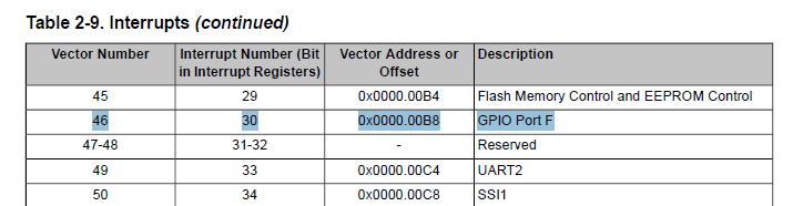
- The datasheet (pg 150) will tell us to use "Register 36: Interrupt 28-31 Priority (PRI7), offset 0x41C" so we will write to memory address 0xE000.E41C (defined as NVIC_PRI7_R) to manipulate Port F's priority level.
- To set Port F's priority, we write "5" to INTC slot (INTA = 28 | INTB = 29 | INTC = 30 | INTD = 31) in Register 36.
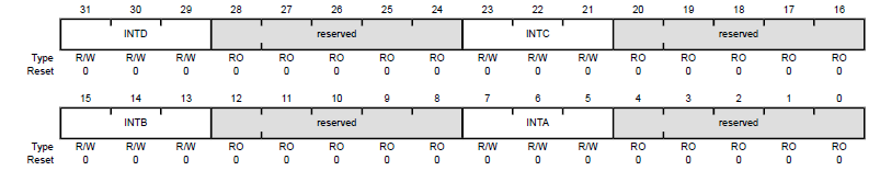
- A priority of 5 is chosen for this example:
- Priority of 5 = [1][0][1][RO] = A (bit 20 is Read Only)
NVIC_PRI7_R = (NVIC_PRI7_R&0xFF00FFFF)|0x00A00000;
h) Enable interrupt 30 in NVIC
- In the Interrupts table (pg 102) we notice that GPIO Port F is Interrupt Number 30. We will use this information to select the correct EN(n) register to write to.
- Since our interrupt number for GPIO Port F is 30, we will write 1 to bit 30 to enable interrupts for GPIO Port F

NVIC_EN0_R = 0x40000000;
i) Clear the I bit
- EnableInterrupts();