-
-
Notifications
You must be signed in to change notification settings - Fork 116
PIO port
Some versions of the PlayStation console have a port on the back labeled "Parallel I/O", pictured here:
The name can be confusing, as it's not an IEEE 1284 printer port, but a proprietary port from Sony, that shares a lot of similarities with the IBM PC ISA bus.
The port was present on all versions of the console, up until the SCPH-900x versions, that removed it.
There is a lot of documentation about this port available online, but this page will be repeating it for the sake of consistency and cross referencing.
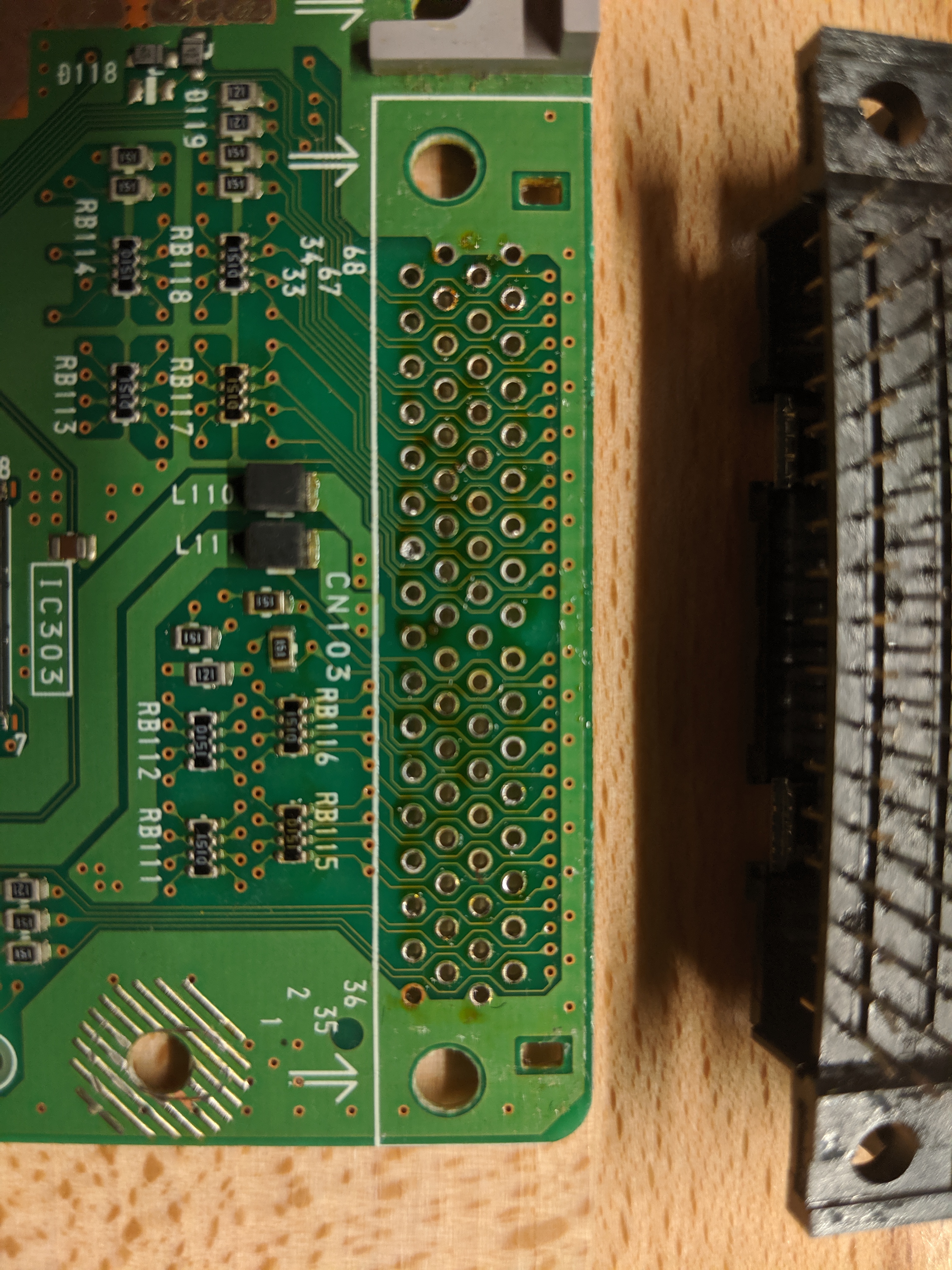
The 68 pins are labeled left to right first, then top to bottom, as pictured:

This pinout is written on the top silkscreen of the motherboard:

Some modifications exist to this PIO port that we will discuss in details. The pinout below takes the known modifications into account.
| signal | number | number | signal | comment |
|---|---|---|---|---|
| GND | 1 | 35 | GND | These are strong ground signals, meant for power distribution |
| !RESET | 2 | 36 | DACK5 | |
| DREQ5 | 3 | 37 | !INT10 | |
| !CS0 | 4 | 38 | !SWR1 | |
| SBEN | 5 | 39 | !CS2 | These are weak ground signals, that can easily be cut to add the SBEN and !CS2 signals |
| D0 | 6 | 40 | D1 | |
| D2 | 7 | 41 | D3 | |
| D4 | 8 | 42 | D5 | |
| D6 | 9 | 43 | D7 | |
| D8 | 10 | 44 | D9 | |
| D10 | 11 | 45 | D11 | |
| D12 | 12 | 46 | D13 | |
| D14 | 13 | 47 | D15 | |
| A0 | 14 | 48 | A1 | |
| A2 | 15 | 49 | A3 | |
| GND | 16 | 50 | GND | These are somewhat weak ground signals, but their proximity to power may be a bad idea to cut and reuse |
| 3.3v | 17 | 51 | 3.3v | |
| 8v | 18 | 52 | 8v | |
| GND | 16 | 53 | GND | These are somewhat weak ground signals, but their proximity to power may be a bad idea to cut and reuse |
| A4 | 17 | 54 | A5 | |
| A6 | 18 | 55 | A7 | |
| A8 | 19 | 56 | A9 | |
| A10 | 20 | 57 | A11 | |
| A12 | 21 | 58 | A13 | |
| A14 | 22 | 59 | A15 | |
| A16 | 23 | 60 | A17 | |
| A18 | 24 | 61 | A19 | |
| A20 | 25 | 62 | A21 | |
| A22 | 26 | 63 | A23 | |
| !SRD | 30 | 64 | !SWR0 | |
| !IN2 | 31 | 65 | !CS5 | These are non-connected signals, that are commonly reused to redirect the !IN2 and !CS5 signals |
| SYSCLK1 | 32 | 66 | LRCLK | |
| BCLK | 33 | 67 | SDIN | |
| GND | 34 | 68 | GND | These are strong ground signals, meant for power distribution |
The architecture of the PSX busses are really similar to that of the ISA bus, and thus share a lot of common features. These common features are the clock, read and write signals, DMA ACK and REQ signals, interrupt line, 16 bits data bus, and 24 bits address bus. The clock is a direct line from the clock signal of the motherboard, and runs at 33.8688Mhz, as soon as the motherboard has power, regardless of the !RESET signal state. All of these signals work exactly the same as described in the ISA architecture.
The main differences are:
- 3.3v and 8v power lines
-
!RESET- this line can be used as an inout, using an open collector. Setting it to ground will reset the console. -
!CS0- unlike the ISA bus, the PSX CPU will indicate it wants to read or write a specific component on its bus using "Chip Select" signals.!CS0is solely used for the PIO port, and no other device on the motherboard, thus a read on the PIO address space with no device connected to the bus will result in a 0xff high impedance read. - I²S audio - the
LRCLK,BCLKandSDINsignals form an I²S input, running in stereo, 16 bits, at 44.1 kHz. It's possible to inject an audio stream into the console's audio output through it. The console drives theLRCLKandBCLKsignals, while expecting audio data on theSDINline.
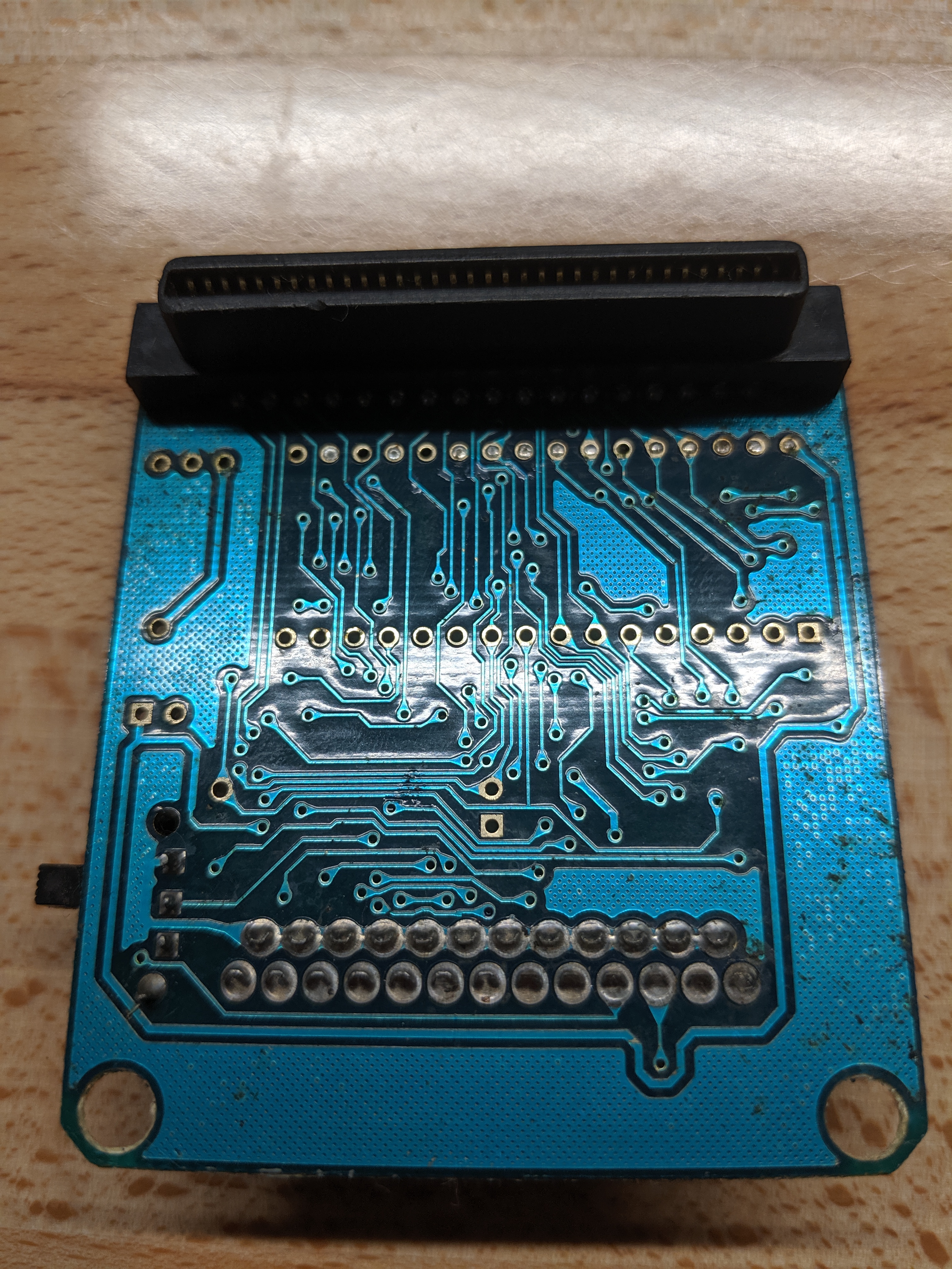
Sony used proprietary connectors for the PIO port, that are loosely based off 68-pins SCSI connectors. The corresponding SCSI connector would be the 68-contact VHDCI connector.
The motherboard connector is made of a mix of metal and plastic, and the cart connectors are usually seen made of plastic. Unlike the VHDCI SCSI connector, they aren't keyed on the sides, making it theoretically possible to plug it the wrong way: the VHDCI SCSI connector is trapezoidal, whereas the PSX connector is rectangular.

There are lots of mating connectors, depending on the manufacturer of the cheat cart. Some variations of the connector still have the diagonal inset at the base, proof that whomever built it was simply reusing the VHDCI design:

The change in the shape from the VHDCI design makes the walls very thin, rendering them brittle and fragile. It isn't uncommon for a PlayStation cart to have its connector broken due to being bent when unplugging.


Interestingly, this design makes it possible to plug a rectangular female cart plug into a trapezoidal VHDCI male connector.
Some effort have been made to try and find replacement for these plugs.
There are many different carts available for the PlayStation that connect onto the PIO port. They all function using the same principle. With the default BIOS settings, the !CS0 line is going low when the CPU tries to access data located at 0x1f000000, 0x9f000000 or 0xbf000000, up to 512KB. At boot time, right after its crt0 is done running, and probably somewhere at the top of its main() function, the BIOS does approximately run the following code:
if (memcpy(0x1f000084, "Licensed by Sony Computer Entertainment Inc.", 44) == 0) {
  ((void(*)(void))0x1f000080)();
}
Then, as the shell is done executing, and has returned to the BIOS to execute the loaded disc, the BIOS does run the following code:
if (memcpy(0x1f000004, "Licensed by Sony Computer Entertainment Inc.", 44) == 0) {
  ((void(*)(void))0x1f000000)();
}
In both cases, this allows a cart plugged on the PIO port to interfere with the boot process, injecting code before and after the shell.
In its simplest form, a working cart for the PlayStation can be a ROM chip connected to the A0-Axx, D0-D7, !RD, and !CS0 lines.
Most carts contain a few more devices however, so a PLA, a CPLD or equivalent logic comparison system is required to multiplex the !CS0 line into the various devices, subdividing the address space accordingly by comparing the proper address lines.
At boot time, the BIOS runs approximately the following code to setup the PIO port:
*((volatile uint32_t *) 0x1f801000) = 0x1f000000;
*((volatile uint32_t *) 0x1f801008) = 0x0013243f;
This can be altered at run time, and have the following meanings: The first hardware register indicates the memory address at which the PIO port starts, and thus is a direct 32 bits address. The second register controls the width of the address bus, the read and write delays, and various other flags.
These are the currently known flags for that second register:
| Bits range | Meaning |
|---|---|
| 0-3 | Write delay - number of cycles-1 to strobe !WR low for. 15 by default on the PIO. A value of 2 seems optimal with modern hardware, giving approximately 80ns of strobing time. |
| 4-7 | Read delay - number of cycles-1 to strobe !RD low for. 3 by default on the PIO. A value of 2 seems optimal with modern hardware, giving approximately 80ns of strobing time. |
| 8 | Recovery period? Off by default for PIO. |
| 9 | Hold period? Off by default for PIO. |
| 10 | Float period? On by default for PIO. |
| 11 | Pre-strobe period? Off by default for PIO. |
| 12 | Access type: 0 = 8bits, 1 = 16bits, off by default for PIO. |
| 13 | Address Increment? On by default for PIO. Disabling this means that a 16 or 32 bits access will be split in 8-bits access on the same address. Can be useful to disable temporarily in order to send large amount of data to an external communication, as sending 32 bits directly is slightly faster than writing 4 individual bytes, as the !CS0 line doesn't have to strobe during the whole 32 bits. |
| 14 | ?? |
| 15 | Extended delay? Off by default on the PIO. |
| 16-?? | Bus width. Default is 19 for 512kB access. Maximum theoretical is 24, thus needs a maximum of 5 bits to hold this value. Actual maximum without changing the base address is 23, or 8MB, as more would collide with the hardware registers themselves. Maybe some of the upper bits of this register are used for DMA. |
